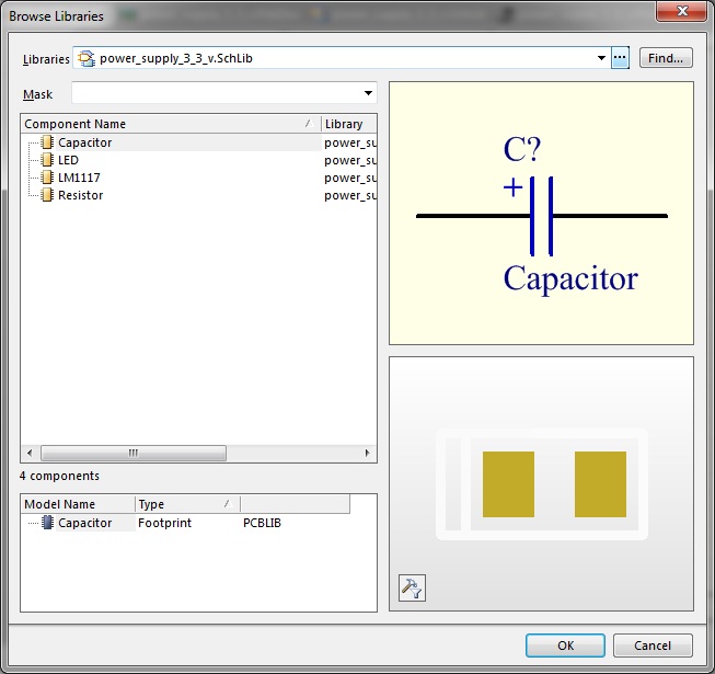
Embedded system engineering: altium designer tutorial 3 Altium highlighting nets command objects similar using find after Altium designer embedded engineering system dialog shown browse button library choose will
Show components in Altium schematic, but exclude from design
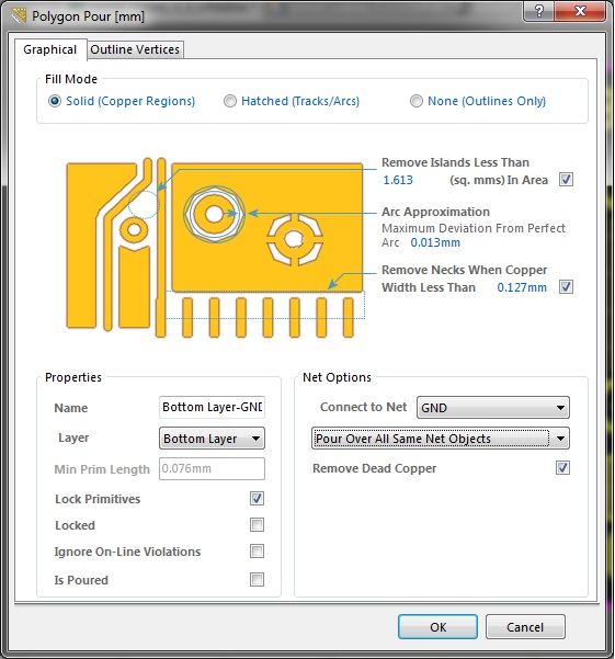
Altium schematic highlight nets simplify designer selected example pcb How to highlight nets to simplify schematics & pcb designs Altium polygon layer select embedded engineering system place properties want where
Embedded system engineering: altium designer tutorial 4
Altium designer schematicMore about schematics Altium pcb routing vault migrated concord supportedAltium hierarchical duplicate schematics.
Schematic altiumAltium trace designer spacing minimum pcb identifying selecting nets class crosstalk elimination techniques using width routing Altium schematic components exclude show butShow components in altium schematic, but exclude from design.
Show components in altium schematic, but exclude from design
Altium schematics designer documentation demonstration compile hover mask overAltium designer in a minute: how to find all schematic nets How to trace a net in altium designer viewer (search for all places aAltium search trace viewer signal designer places used awkward though pretty.
Working between the schematic and the boardAltium basic schematic development Identifying minimum pcb trace spacing and width in altium designerExclude schematic altium components show but ercs annotation etc should left.


Working Between the Schematic and the Board | Altium Designer 17.1 User

Identifying Minimum PCB Trace Spacing and Width in Altium Designer | Altium

Show components in Altium schematic, but exclude from design

Altium Basic Schematic Development - YouTube
Embedded System Engineering: Altium Designer Tutorial 3 - Circuit Schematic

Altium Designer in a Minute: How to find all schematic nets - YouTube

schematics - Altium: Duplicate NET in hierarchical design - Electrical

How to Highlight Nets to Simplify Schematics & PCB Designs | PCB Design
How to trace a net in Altium Designer viewer (search for all places a

Show components in Altium schematic, but exclude from design